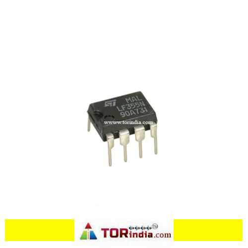
JFET Input Stage: Features a high input impedance JFET input stage, which results in very low input bias and offset currents.Low Input Bias Current: Typically around 30pA.Low Input Offset Voltage: Generally around 2 mV max, with low drift.Wide Gain-Bandwidth Product: Offers a bandwidth of 2.5 MHz.High Slew Rate: Possesses a high slew rate of 5 V/µs.Low Supply Current: Designed for low power consumption, typically around 3.6 mA or 4 mA, making it suitable for battery-powered and portable devices.Internal Frequency Compensation: Includes internal compensation to ensure stability.Offset Voltage Adjustment: Allows for offset voltage adjustment without degrading drift or common-mode rejection.High Common-Mode Rejection Ratio (CMRR): Offers a high CMRR, typically 80 dB or 100 dB.