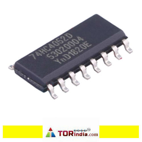
It contains two independent 4-channel analog switches.Wide Analog Input Voltage Range: Can handle analog input signals from -5 V to +5 V.Low ON-Resistance: Minimizes signal loss through the switch. Typical ON-resistance values are:80 ? (typical) at VCC - VEE = 4.5 V70 ? (typical) at VCC - VEE = 6.0 V60 ? (typical) at VCC - VEE = 9.0 VLogic Level Translation: Enables communication between 5V logic and ±5V analog signals.High Noise Immunity: As a CMOS device, it exhibits high noise immunity.CMOS Low Power Dissipation: Features low power consumption inherent to CMOS technology.Break-Before-Make Switching: Designed with a typical "break-before-make" action to prevent momentary short circuits during channel switching.Enable Input (E): A common enable input (active LOW) for both switches. When E is HIGH, the switches are turned off (high-impedance state).Digital Select Inputs (S0, S1): Two digital select inputs are used to choose which channel is connected.Input Clamp Diodes: Includes clamp diodes on the inputs, allowing the use of current-limiting resistors to interface inputs to voltages exceeding VCC.ESD Protection: Provides robust ESD protection, including HBM (Human Body Model) exceeding 2000 V and CDM (Charged Device Model) exceeding 1000 V.Wide Operating Voltage Range: Complies with JEDEC standards JESD8C (2.7 V to 3.6 V) and JESD7A (2.0 V to 6.0 V). It can operate from 2V to 10V (single supply) or ±1.5V to ±5V (dual supply).Wide Operating Temperature Range: Specified from -40 °C to +125 °C.